Monday, April 4, 2011

Going up to 13cm W1GHZ rover modified transverter

The first thing that discourages builders around the Europe from building the W1GHZ transverters is the different band plan on the 13cm and 9cm. Moreover some countries can not even operate on the 9cm band. Some counties, like Croatia can use the both portion of the band (2304 & 2320 up to 2450 MHz) but all activity is concentrated around the 2320 MHz. Using the originally designed oscillator is not of much help. The problem can be solved using the lately wide spread oscillators based on the Si4133 synthesizer with direct  L.O. frequency for the 23cm and 13cm bands. The oscillator can generate the frequencies between 400 and 1900 MHz what he is OK for the 432 MHz I.F. on the 13cm band. Of course, this is no more simple and cheap project, but just an option for the builders. The one I have is coming from Australia, offering 16 different pre programmed frequencies, with possibility to reprogram any required frequency in the mentioned range with the step of 1 MHz. DEMI is offering their version (ApolLo) of the oscillator based on the same synthesizer.


As I plan to use this synthesizer for another 6cm transverter project, the same was replaced with the old fashioned L.O. based on the crystal oscillator with the chain of multipliers. Already proved S53MV oscillator design, the same one in use in the 23cm simple beacon, was assembled also for this project. After choosing the I.F. of 432 MHz, the required L.O. frequency was 1888 MHz. Approach was simple, first generating the signal of 629.333 MHz and than multiplying the same to 1888 MHz. The oscillator multiplying factor is 36 (3 x 3 x 2 x 2) with the crystal oscillating on the 17.481 MHz. This is where all your odd frequency crystals  ripped out from the old service mobile radios are coming handy and finally useful. If you have an inventory list of all your crystals you will have in no time the right one ready. If you do not have the list, you will have in no time your fingers dirty digging out for the right one :-) .


The final VXO oscillator frequency can be tuned quite wide, so the crystal frequency does not have to be exactly as the required one, making easier to look for the right one. After a minute or two the frequency is very stable despite the the big multiplier factor. The same principle and oscillator was used in many projects. The first 720 MHz oscillator for the 23cm rover transverter was the same one. Multiplying the 20 MHz crystal from the old hard disc was easy. Multiplying the 18 MHz computer grade crystal was used in the 23cm simple beacon project and  the next 13cm rover transverter will have the same oscillator.


Driving directly the transverter board with the 629 MHz seems to be a nice idea, but I was not sure that 1" pipe-cap filter can tune efficinetly down to 1888 MHz. Some experimenting and tuning was required on the pipe-cap filter and for that reason I decide to use another (no tune) multiplier. The S53MV Beacon 99 script is full of designs that can be used for such multiplier. I decide to use the oscillator multiplier from the ZIF SSB transceiver for the 9cm band (3400 MHz). The same article is also showing the oscillator that I am using for most of my simple projects.I knew that the filter in the multiplier chain is designed for the 1700 MHz, but I expect not so sharp filter response due to the design. The original design suffer a minor modification on the first stage where ATF35376 was replaced with the simple SNA-386 mmic from Sirenza. I just don't like this HEMT devices.Of course, the bias network was changed as well and the gate resistor was removed also. Idea was to saturate the MMIC to get enough harmonics, filter the 3rd one and amplify the 1888 MHz signal with the BFP420 transistor. I drive the SNA-386 with the 6dBm from the 629 MHz oscillator. At the end I was happy with the 14dBm of the signal on the 1888 MHz.


The multiplier was assembled on the 0.8mm FR4 laminate where no tuning was required. After the initial tests the SMA attenuator was replaced with the SMD resistor network just before the SNA-386 on the PCB. Vias required for the MMIC and BFG420 grounding are replaced with the grounding done by drilling the 2.5 mm holes filled with the melted solder wire. The ground side of the PCB is covered with a peace of thin copper foil soldered for the PCB creating a good connection with the pins.


Once I had the oscillator and multiplier ready and running properly the rest was easy. As I ordered a few rover PCBs it was just about following the Paul's procedure. There was no need to solder the original multiplier part with two pipe-caps just the part from the mixer and the front end. First, two 1" pipe-caps were soldered using the flat iron technique and they are separately tuned to 2320 MHz using the procedure explained in the 13cm Pipe-cap filter post. Soldering the pipe-cap may be tricky if you are using just a low power soldering iron. On the other side if you are using high power iron, the job may look ugly and the PCB can be damaged as well. I prefer to preheat the pipe caps on the flat iron and to position one by one using the tweezers on the marked place on the PCB. Than you can use your standard soldering iron to properly solder the pipe-cap for the ground side of the board. Soldering the RX and the TX front was quick and the only thing you have to care is the position of the MMIC blocking capacitors. I was short of MGA-86567 and instead I install the MGA-86563, the first I found in my drawer with the similar characteristics. The PCB is just enough small to fit SOT-363 (SC-70) surface mount package.


Connecting the L.O. and a FT-817d with the transverter board with a peace of semi-rigid coax was enough for the first RX test. Everything was looking OK and the MMIC current was by the specs. I checked the rx part tuning the filter pipe-cap to the maximum signal transmitted using the alias frequency from my  AD9951 DDS oscillator. To check the TX side i just insert the 25dB attenuator before the mixer I.F. port and the TX was pushing out 40 mW. It seams that Sirenza SNA-586 was running by the specs. delivering the max. output P1dB power. Initial tuning with the antenna was with the transverter assembled in the old PC switching power supply.


Just a small power amplifier using the AH-102A MMIC delivering almost 27 dBm of power is hiding bellow the orange heat-sink This will help to check the TX part running some more power to the antenna. This setup can not be used outdoor, so another w/tight housing was prepared with more room to accommodate a bigger power amplifier. The same one can be mounted on the mast, just behind or close to the antenna to reduce the loss of the signal in the coaxial cable. Looking from the top, there is a 629 MHz oscillator followed by the x3 multiplier stage. Below the multiplier there is well known transverter board. From the TX SMA connector on the left side the semi-rigid cable is connected to the power amplifier while from the RX SMA connector the semi-rigid is connecting the commercial 13cm 25dB preamplifier. At the bottom the coaxial relay is connected to the amplifiers and the antenna connector. Dummy proof sequencer is positioned on the left side of the housing assuring the carrier or PTT operating mode.

 
The transverter was tested from the home and the portable location. With only 450mW and 90cm dish antenna with the WA5VJB log. per. feed the contacts up to 250 km were established during the winter time. The summer will bring more activity, better propagation and some ducting as well. The video is showing the 200 km qso on 2320.100 MHz with the Italian station. 13cm band was used as a talk-back frequency trying to establish the contact on the 10 GHz.


Job remained to be done before the summer microwave season is to replace the noisy commercial preamplifier with the latest AD6IW "state of the art" uW LNA followed by the 13cm bandpass filter. The left side of the w/tight housing is leaving enough space for the 6 watts power amplifier. After that the transverter will be ready some DX-ing on the 13cm band. Latest AD6IW uW LNA ready to be inserted:


 The same principle will be used for the 9cm W1GHZ rover transverter. Oscillator is almost ready and the original multiplier on the transverter board will be used, avoiding the extra multiplier.

Saturday, March 12, 2011

Yet another W1GHZ rover transverter modification

After several successful modification it was necessary to unite all in one project. The transverter was tailored according to the parts that are found in the drawer, and some improvements are possible indeed. The PCB is a copy of the original W1GHZ project with a few minor modifications. As seen in the diagram, another type of mixer (RMS-30) was used. The MMIC on the RX side was replaced with the INA-02186 and lately with the MAR-6. The output MMIC ERA-5 was replaced with SNA-586 and the resistor combiner/splitter was replaced with the PIN diodes.


The first thing you notice is that the PCB is almost half size because there is no L.O. multiplier included. Instead of that there is just a SMA L.O. port connector so IF of 144 or 432 MHz can be used with the appropriate external local oscillator ( 1152 MHz or 864 MHz). The RMS-30 mixer has a slightly different pin-out so small modification was required also here. The top PCB TX side remained untouched, together with the part where PIN diodes are inserted. The PCB RX side is slightly changed, now allowing 2 MMIC on the RX side if required.


The PCB bottom side is mainly the ground layer. The PIN diode modification was done mainly on the bottom side. The splitter resistors are replaced with the diodes and a holes for the wires are drilled through the board connecting both PCB sides. After that at the bottom side, the pads are cut with the sharp X-Acto knife creating the soldering pads for the PIN diodes network (resistors, coils and the capacitors). The outcome  is higher isolation between the ports and lower loss comparing to the resistor splitter. The PCB tracks are then extended to the RX/TX power supply pads allowing the switching using the same voltage.


The transverter was ready for the test. Connecting the external L.O. ( 864 MHz ) and the IF radio ( 432 ) Mhz the RX part was tested first. Immediately, there was a high noise on the RX side indicating that the RX part is oscillating. Adding a few extra via to the MMIC ground pads helped a little bit but under the some conditions the INA-02186 was oscillating again. The known problem was not easy to solve, the 1.6 mm FR4 was too thick for INA-02186. At the end the RX MMIC was replaced with the MAR-6 with surprisingly good result.


It's true that MAR-6 can give us less gain and higher NF comparing with the INA-02186 but the transverter is very stable, not showing any sign of self oscillations under various conditions. Housed or not, with or without the extra LNA on the input, with the high input signal the MAR-6 was a simple solution for the home-brew PCB with via done by simple wire. The TX side of the transverter performed very well after the first test. All the MMIC voltages were according to specs. and no sign of oscillations were noticed. The output power is 40 mW.


The transverter was tested with the IF drive of 1 mW on the 432 MHz from the FT-817nd through the 50 ohms attenuator and with the 6 mW of L.O. power on the 864 MHz. The signal was clean and stable. Both the transverter and the L.O. were housed in the box made from the scraped nescaffee can metal sheet. The final version can be built without the numerous SMA connectors using just the semi-rigid teflon coaxial cable for connecting all parts of the transverter. Using so many SMA connectors can be costly and some builders don't have the access to e-bay or any other possibility to buy the connectors. At the end, the idea was to build simple and cheap rover transverter. 
On the other side, the modular approach will allow us to build and test all units separately avoiding the headache when trying to resolve the problem on the finished not working transverter what can be very important for inexperienced builders. More over, this approach give us the possibility to experiment with the various L.O., LNA, final power amplifiers, changing the set up very quickly and choosing the right one.


Various test were performed with the transverter to assure that all is working properly. On this video you can see the RX part receiving the beacons ( lower signal are beacons 100 and 250 km away). The strong signal is the 1 watt local beacon running on the 50 ohm dummy load located in the next room not more than 10 meters away. The noise appearing every 10 seconds is the AN/FPS-117 radar running some 30 km from the location with the clear LOS. Inserting the sharp response 23 cm filter before the front-end did not improve the situation because this is the in-band disturbance. The RX MMIC was just a MAR-6 so don't worry to much especially if you plan to use extra LNA on the RX side. The antenna was just a simple 25 el. loop antenna.


The second video is showing the same setup but with the YU1AW LNA using the BFG-540x as active component. Even not screened the LNA and the transverter performed excellent showing no sign of instability. Adding the LNA I improve the overall NF and a total conversion gain. The same beacons signals were checked. It is not easy to notice the difference on the video due to the local QSB but improvement is obvious.


Presented modular approach give us the possibility to use different L.O. with the different I.F. radios to reach the 23cm band. 144 or 432 MHz or some other I.F. depending on the radio you have requiring the proper L.O frequency. For the L.O. we can use the PLL, DDS, or some other way of generating the signal, today quite popular Si4133 with the possibility to program any frequency from 400-1900 Mhz in 1 MHz steps. Bearing in mind the simplicity of the rover transverter project I choose the old fashioned crystal multiplying chain starting with the 96 MHZ crystal. After multiplying, the final frequency was 864 MHz. This frequency constrain us to use 432 MHz for the I.F. which is simple but not the best solution considering the well known mixing products problem when using 432 MHz for the 1296 MHz I.F. Anyhow this is more acceptable than running the 1440 high side injection with the reverse 144 MHz LSB tuning. Most of the radios are blocked and can not even tune below the 144 MHz and other suffer with the lover sensitivity out of the band. The good thing is that the filter response is also better if we use the 432 MHZ I.F.
The simple and good oscillator chain is basically S53MV 23/13 cm transverter oscillator with the simple modification. Instead of the original 576 MHz oscillator following the 96-288-576 MHz chain I tune just the last multiplier to achieve the 96-288-864 MHz chain. The signal was clean and stable, power 6-7 mW. If you prefere to use 144 MHz (right side up) for the I.F. than the same 576 MHz oscillator can be used adding another multiplier stage to reach 1152 MHz.


At the end just a brief report regarding the cheap relay that Paul is using with the rover transverters for the antenna switching. During the last year Friedrichshafen HAM flea market I get the surplus aluminum milled box with 5 SMA connectors, several MMIC, smd directional couplers and other handy parts including 2 peace of the OMRON G6Y-1 relays, all that for just a few Euro. The unit was part of 900 MHz GSM equipment. It is true that this relay was the 5 volts type but at the end this was the advantage because we are using 8 or 9 volts for our transverter RX/TX stages.


Relay, 78L05 voltage regulator, 2 smd blocking capacitors, 1N4006 protecting diode, a peace of 0.8mm FR4 and 3 SMA connectors will give us the coaxial relay able to handle 10 watts of the RF power (sequenced) on the frequency of 1 GHz with the I.L. of 0.5 dB. Not bad at all! The double side 0.8 mm FR4 PCB was tailored where 50 ohms tracks are cut with the X-Acto knife. SMD blocking capacitors are soldered on the bottom side just close to 78L05 pins, together with the relay protecting 1N4006 diode. Even lower I.L. can be achieved soldering the coax directly to the PCB without using the SMA connectors.

So, that's it ....

Monday, February 14, 2011

Simple beacon for 1296 MHz - S53MV design

Not so many beacon articles can be found on the web where everything is well explained and documented regarding the home-brew beacon design for the microwave frequencies. One of the authors who really care about it is Matjaz Vidmar S53MV. All his projects are well described, proven in practice, and all assembled from the cheap and wide spread electronic parts. The most important, they are working !


Between all of his numerous design, the beacon for the 23 cm band is one of the simplest microwave project. The project was published years ago and can be found in the script "Beacon 99" (PDF format) on the following address: http://lea.hamradio.si/~s53mv/beacon.pdf .
The design is straight forward, 648 MHz oscillator and 1296 MHz multiplier with small amplifier. All beacon was assembled on only two 0.8mm FR4 PCB. The oscillator PCB is single side and the 1296 MHz doubler PCB is double side with one side used for the ground. If you strictly follow the design and instructions there should be no mistake. The 1296 MHz multiplier is a no-tune design, so plug and pray. The 648 MHz oscillator board consists of the chain of multipliers where each one should be tuned to the exact frequency to obtain the good signal on the output (10dbm).

The multiplier chain is simple :
Oscillator 27 MHz
x2 multiplier 54 MHz
x3 multiplier 162 MHz
x2 multiplier 324 MHz
x2 multiplier 648 MHz


As I already build the 648 MHz oscillator for the 1296 ZIF SSB TRX (in the same script) I decide to use this one for the beacon with the main crystal frequency on 18 MHz. The signal on 648 MHz was stable and the power was higher than 10 dBm. Frequency can be adjusted through the multi turn trimmer feeding the voltage to the varactor diode. With the cheap computer grade 18 MHz crystal the range 1295.900 - 1296.100 MHz was obtained with no problem and stable output power and frequency. Attention should be used when tuning the trimmer capacitors. Each multiplier stage, from the oscillator upward, should be tuned to the maximum power at the same time controlling the frequency of the multiplier stage that we are tuning. That way no mistake can be done and you should end with the correct output frequency.


The 1296 MHz multiplier board is a no tune, so after connecting the power you should have 23 dbm (200mW) output power. Also here, I did not follow the design because that time I did not have all parts ready. So I apply some modifications:
Instead of the 1st ATF35376 (multiplier) a MMIC SNA386 was used, modifying also the bias network. Both gate resistors are removed together with the LED diode with 330 ohm resistor and 10 ohms resistor was replaced with the 240 ohm. Standard MMIC multiplier configuration was used to double the frequency from the 648 to 1296 MHz. There was enough drive power to saturate SNA386 and to generate strong harmonic on 1296 MHz.


Straight after the 4 pole strip line filter the first amplifier ATF35376 was again replaced but now with MMIC ERA-2. Gate resistor was removed and MMIC bias was adapted for the 12 volt supply. 4V7 diode was removed together with 180 ohm resistor and 10 ohm bias resistors replaced with 220 ohm.

Of course, to complete the modification, the last amplifier BFP196 was replaced with the BFG540x transistor amplifying the signal to the +23dbm output with the power supply of 12 volts.


Just a two things to take care when building this multiplier, the grounding MMIC and the output transistor via are just 3.2 mm holes closed from the ground side by thin copper foil. Tho holes are then filled up with the hot melted tinol creating good contact with the copper foil. Four filter stubs are grounded using the 0.6mm silver wire (one wire from the RG-214 center conductor). Bend the wire creating the C shape to allow good connection (2mm) on he top and the ground side of the PCB. Tight the wire with the pliers and solder the wire both sides.

A short troubleshooting list if you run in the problems:
- BFX89 transistors should be mounted as close as possible to the PCB, not more than 1 mm above it
- BFX89 can be replaced with the BFY90 with better results
- BFR91 transistor is soldered directly from the copper side
- 22 nF blocking capacitors a very important, use the good quality ceramic capacitors
- keep all connecting leads as short as possible, a must for the capacitors
- the coils L4 and L5 are identical, pay attention on direction
- use only high quality trimmer capacitors in the multiplier chain
- up to now I build several oscillator boards for the frequencies of 576, 648, 720, 864 MHz and the only problem I had was the trimmer capacitor. After some time, the low quality trimmers are changing their value. The tuning point may be quite sharp on the second and the third stage, so this can cause that your oscillator after some time stop working, more often if your beacon is located outside, on the mast close to the antenna.

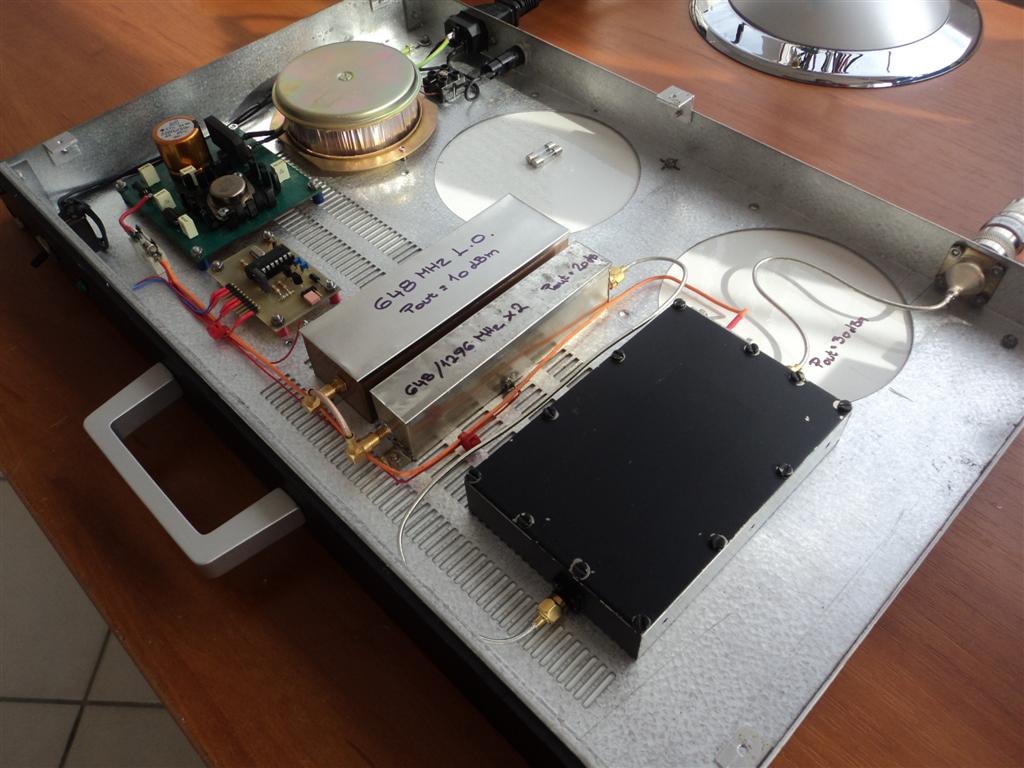
The proper shielding is required as per article instructions and the beacon can be mounted close to the antenna to avoid the loss in the coaxial cable. The keying is done by means of switching the power supply to the 648/1296 MHz stage. The oscillator board is always powered to achieve the better frequency stability.


I prefer to have the beacon not exposed to the atmospherics. The frequency stability is also less affected by the temperature if the beacon is held indoor. Of course, the loos in the coaxial cable have to be covered by extra amplifier to have the same power on the antenna. My beacon was built around standard 1H 17" rack together with the power supply and the IK0WRB beacon keyer. The keyed voltage is little bit lower than 12 volts. This result with the lower power output (100mW), but also the final transistor lower temperature. In the rack there is enough place for the extra amplifier and the inter-digital filter if required.


I was surprised with the final frequency stability and the shape/sound of the signal. On the video, you can notice the second harmonic frequency received on the FT-817d accompanied with the W1GHZ 23cm transverter (high side injection). Keyed signal can not be noticed due to 50 ohm termination, and the frequency stability is not affected by the keying of the final stage. At the same time notice the power output on the power meter. The beacon was left on the bench for a couple of days connected to the dummy load. No significant change of frequency was noted nor the lower output power.


After the initial beacon connected to the dummy load test, there was time to perform the "live" test running the beacon connected to the real antenna. The first antenna that I have handy and ready was the "Cheap WA5VJB" style yagi antenna. With some 10 dBi gain and indoor, connected to the beacon with a peace of RG-214 cable the antenna was pointed to the nearest mountain (1400 m ASL) from my home location. The idea was to use the already well known reflection point on the top of the mountain so the beacon can be heard in the near Italian provinces. The signal was good and stable, with no significant frequency drift. After several initial reports the beacon was switched off, ready to be mounted on the remote location.


The beacon is planned to be mounted indoor, so quite long run of the coaxial cable will result the low power on the antenna with just a little bit more than 100 mW of the beacon output power. For that reason I add another 10 db amplifier stage at the end easy producing more than 1 watt of output power. The amplifier was mounted in the robust CNC machined aluminum housing attached to the bottom of the rack.


The final result can be heard on the following video clip. Of course, 9A4QV/b signal is the strongest one between the two others.


Thursday, February 3, 2011

W1GHZ 1296 MHz Hairpin filter


Building the Rover transverter for the 1296 MHz I experience the lower power output than expected, so I start looking what can cause this 10 dB lower output than predicted. Not only on the TX side, I notice the lower signal also on the RX side comparing the received signal with the other transverter design with the similar conversion gain. Among the all other parts affecting the signal loss, the filter is the only one that was designed and not fabricated. Paul, the author already made a good job with all relevant measurements on the filter, already published, but I wanted  some other verifications to get some more data to be able to use the same filter in some other projects.


The filter was duplicated from the W1GHZ 1296 MHz transverter (3 pole) on the standard 1.6mm FR-4 laminate. I prefer to use the "toner transfer" technique with my flat iron. Iron already became the standard tool on my workbench :-) A pair of SMA connectors are added to be able to measure and compare the filter more easily. Of course using the SMA connectors bring some additional losses to overall measurements, but I can live with that. The filter itself in the transverter configuration will have even lower I.L. 

IMPORTANT !!! The following measurements are done with the reference signal of -12.72 dBm !!!

So the reference signal was not 0 dBm, but -12.72 dBm and it is necessary to correct all the readings that you see on the following spectrum analyser screen shots. I start with the center frequency (C.F.) 1296 MHz, span 500 MHz to see quickly if my flat iron was successful or not :-) Quick look on the curve and everything looks as predicted. The filter is centered around the 1296 Mhz with the I.L of -4.53 dB (17.25dBm -12.72dBm). Looking the screen the BW - 3dB is 100 MHz.


The next step was to measure the filter response 144 MHz from the center frequency. At 1152 Mhz the signal was 40.28 dB down as per screen shot. I forget to measure the signal on 1440 MHz but we can see that the skirt is not so good as on the lower side, so the signal is only 23.28 dB down on the 1440 MHz. Of course "Right side up" mixing approach should work better than using the higher L.O. frequency in this case.


As I plan to use the same transverter but with the I.F. 432 MHz I measure the filter response on the 864  MHz with signal  62.28 dB down. The center frequency is 1296 MHz and the span is 900 MHz, 10dB/div. Despite the mixing products problem using the 432 MHz for the I.F. transverter is working quite good with this filter.


Using the same filter with the I.F. of 50 MHz to work on 1296 MHz is almost impossible. The signal on 1246 MHz is down only 11.28 dB. This measurement was just to compare this filter skirt with some other filters measured before. So here is the screenshot.


When measured the filter bandpass and the loss, I was still curious about the filter return loss / SWR so additional test was performed using the network analyser. This measurement gave me quite good idea about  the characteristics where the minimum obtained R.L. was 16.29 dB or the SWR of 1:1.36. This way I was quite sure that the mixer RF port is terminated with the impedance close to 50 ohms.


At the end, I tried to tune the filter for even better RL, what was possible but on the other side affecting the pass-band characteristic. This filter is designed as a no tune project and I was happy with the above presented results. They correlate much with all already published by Paul, W1GHZ. The small differences are result of  maybe different FR-4 used, slightly different dielectric constant, or the fact that my filter was not covered - galvanised. Non uniform Er can also affect the results where FR-4 has quite loss on microwave frequencies. Of course, the "Right side up" version of the transverter is using the 4-section hair pin filter with little bit different characteristics, but why not believing to Paul who already made all relevant measurements.

To summarise:

Freq:   1296   1152   1440   1246   864     MHz
Loss:   4.53   40.28   23.28  11.28  62.28  dB


Wednesday, January 26, 2011

3cm Waveguide double-slot antenna

Omnidirectional, horizontally polarised waveguide antenna for the 3cm band that can be used for ATV or beacon operation. This is not the beginners project as it requires some special machining tools, or CNC equipment . On the other side the software and calculations can be useful for the lower band antennas (23cm or 13cm) where hand-tool can be used to fabricate waveguide antenna.

All calculations are done using the HLSSA software running properly also in the DOS window. Using the  WR-75 size waveguide, 10 slot per side with the central frequency of 10.450 MHz, gain of 12 dBi was calculated.


Actual antenna dimensions are then modified to meet the calculated ones. The calculated distance Slot-Short (Lwg/4) was 11.29 mm, but I prefer to use 3 x Lwg/4 and adding the 2.3 mm length for the short-end cap give us a total length of 36.17 mm. If the short-end tuning is required, it is easy to insert the sliding short-end peace when you are using 3 x Lwg/4 length. With only Lwg/4 length, there is not so much room for tuning the antenna for the best RL.


For easy tuning and troubleshooting there is no coaxial to waveguide transition on the antenna. Instead, the WR-75 size flange was attached. To test or measure and tune the RL/SWR of the antenna the commercial or previously checked and measured coax to waveguide transition should be used not to affect the RL of  the antenna itself.


If you are planing to use the antenna indoor or on the location protected from the rain fall or snow than no radom is required. If you are planing to use the antenna positioned outside, on the mast, than good microwave radom should be used to protect the antenna from the watter but also from the bugs that just like to settle inside the waveguide. The radom should be at least 6cm in diameter not to degrade the basic antenna characteristics. Do not use the heat shrink tubing or similar ideas other then microwave radom. Anything in the near field region of the antenna can spoil the gain, diagram and overall characteristics. If you are constrained to use this kind of antenna protection, than insure that the same is inserted in the HLSSA program during the antenna designing.


The last attached photo can give you some idea how to install the antenna without radom. When installing the antenna, pay attention to position the antenna vertically. 3dB vertical beamwidth is quite narrow !! More slots will give you more gain but the vertical beamwidth will be narrower. If your antenna is positioned very high , on the hill comparing to the close stations, the close stations may suffer the narrow bandwith problem. If the antenna is slanted, this problem will affect some users even more.
Another fact is that the omnidirectional diagram is not the perfect, to be honest, far away from the perfect becoming more like cross diagram with the regions with the difference of 3dB comparing to the maximum antenna gain. So if you want to cover your preferred areas, turning the antenna can give you sometimes even 3 dB more gain. This problem can be solved by using the "wings" attached to the antenna, already published on the web.

Saturday, January 22, 2011

3cm Waveguide to SMA transition

Not so easy to find now days and if new, sometimes quite expensive, the waveguide transition became the target of many home-brewers. So many different dimensions and designs are published with the same idea of making a good waveguide to coax transition.
If you have the possibility to measure the RL and SWR than almost any design can be tweaked for the best results, but if you can't measure it than you have to rely on the data provided by the author or constructor. The transition that I built, based on the Paul W1GHZ article was easy to copy, without any fancy tool and tuning equipment. I prefer to use his design because there are only two measures that you have to take care of while all others dimensions are defined by the standard waveguide size.

To build this transition we need a peace of WR-75 or WR-90 waveguide with the flange, SMA female connector, and a peace of the brass or copper sheet. Cut the peace of the required waveguide length, but not shorter than 1 lambda. Drill the hole for the SMA connector from the short end of the waveguide (distance C). Distance is measured from the end of the waveguide to the center of the pin hole. Hole should be 4,2 mm in diameter if you are using standard SMA connector with the teflon insulation. Find the female SMA connector with the longer pin/teflon insulation and put the same in the prepared hole on the waveguide. From the closer waveguide end cut the excess teflon inside the waveguide so only center pin will remain like on the picture below. The diameter of the center pin is 1,27 mm and the only thing you need to do is to cut the pin exactly according to the length D. This is the pin length in the waveguide!! Finally, cut the peace of the brass or copper sheet to form short end cover for the waveguide (AxB dimensions).


W/guide       A        B       C      D
WR-75     19,05  9,525  5,26  5,49
WR-90     22,86  10,16  5,46  5,89
(all measures in mm)

Now when we have all parts ready, it's time to put all this together. Of course, we will need to solder the short end peace to the waveguide and then the SMA connector in the previously prepared hole. This can be done by using the high power soldering iron or gas torch with not so tidy result. I prefer to use the iron, the same one I am using for tone transfer PCB. With the highest temperature set after 5 to 6 minutes the parts will be hot enough to work with them. Using the pliers, rotate the waveguide vertically with the flange sitting on the flatiron and with the other set of pliers position the short end on the waveguide end. Use the standard soldering iron to solder the short end. While the waveguide is still hot, position the SMA connector on the place and use the same technique to solder the SMA.


After the job is done, leave the waveguide to cool down for a few minutes. I make a several transitions using the same technique and the results are quite good. The RL obtained is -20dB (SWR 1:1.2) which is not bad for no-tune version. You may get lucky to get better results but if you are looking for lower SWR than you have to tune the transition. This can be done using different techniques: by changing the short end distance or even by adding some tuning screws. AD6IW give me a hint how to do this easy way. Making the hole for the SMA bigger (lonitudinally) we are able to change the distance from the pin to the short end by moving the SMA along the waveguide. Find the position where the SWR is lower and then solder the SMA. This will be good enough for all amateur applications.


After all, one hour job can give you a nice waveguide transition. To bulid or to buy, it's up to you...

Monday, December 27, 2010

Beacon keyer IK0WRB

http://web.tiscalinet.it/vcoletti/pic/keyer/beacon.html

If you ever build the beacon, or if you have the idea of building one, there is a part that every beacon needs, the keyer. Various beacon keyer designs are available on the internet but IK0WRB solution was the one that I prefer to use. Up to now I built a several keyers and all of them a working perfectly. As a matter of fact, the 144 MHz 9A0BVS beacon is running more that 3 years with this keyer where small reed relay !! is switching the power for the buffer stage. At the beginning nobody believed that the relay will last so long. It is still working.

As a spare solution, there is a keyer based on the transistor switch, where no mechanical parts are included. The schematic is standard IK0WRB keyer with a small modification where two transistors are used in a switch configuration. The first NPN transistor is used to key the input to the ground, and the second PNP transistor is used to switch the positive voltage. The jumper is used to chose beteween this two options, depending on the type of the beacon you are planing to use.

One of the things that make this project unique is the possibility to change the text and the format of the message on a very convenient way, just by tweaking the options in the windows based application written  by the author. The same application is generating at the end the HEX file to be programmed in the PIC 16F84. Of course, the message speed and the duration of the beacon carrier can be selected. Another nice feature is the possibility to use any convenient crystal frequency for this project. As I have a bunch of standard 3.579 MHz crystals, this is my favorite.


All the project can be done using the SMD technology where complete PCB can be really small. Between using the tiny SMD components and drilling the holes on the PCB for the standard components I prefer to use the SMD :-) . As this can be a beginner's project I made a PCB using the standard components with the socket for the micro-controller where the same can be easily reprogrammed with the new messages for a different beacons.


The keyer from the photo is a part of the 23cm beacon where positive voltage is keyed for the 648>1296 frequency doubler. The shape of the signal is looking good without any clicks or chirp. Simple keyer for all beacon builders....